The AI landscape is undergoing a radical transformation with the emergence of custom AI chips, heralding a new era of performance and power efficiency. Specialized silicon solutions are defining this shift, achieving up to 300% more efficiency than traditional GPUs and setting new standards in tasks such as inference for large language models.
Redefining AI Performance: The Rise of Custom Chips
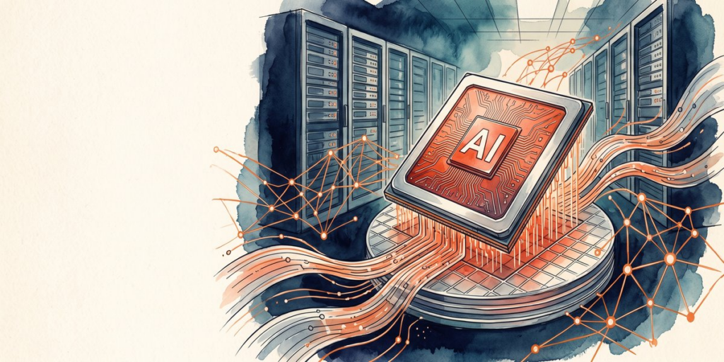
The “Custom Silicon Revolution” within artificial intelligence chip development marks a pivotal shift towards achieving unparalleled advancements in processing capabilities and energy efficiency. This revolution is largely propelled by the advent of custom AI chips, such as Google’s Tensor Processing Units (TPUs) and Intel’s Gaudi series, which have significantly altered the computational landscape for AI workloads. Unlike traditional graphics processing units (GPUs), these custom silicon chips are meticulously engineered to cater to the unique demands of large language models (LLMs) and intricate neural networks, setting new benchmarks for AI processing performance.
One of the most striking examples of this shift is Google’s Ironwood chip, which has demonstrated the capability to reach ExaFLOPs of performance. This level of computational power is essential for tasks involving LLMs, offering a substantial leap over traditional GPU-based solutions. The specific design and engineering of custom AI chips allow for a better fit for the parallel processing requirements of AI and machine learning algorithms. This specialization not only boosts computational throughput but also enhances efficiency by tailoring the chip architecture to the task at hand.
Furthermore, Field-Programmable Gate Arrays (FPGAs) have emerged as a versatile and powerful solution in the realm of custom AI silicon. By providing a customizable hardware accelerant, FPGAs enable more tailored computation that aligns closely with specific AI workloads, thereby offering marked improvements in both performance and energy consumption. For instance, Positron’s Atlas system, which employs FPGA technology, showcases a 70% speed enhancement over Nvidia’s multipurpose GPUs for transformer model inference tasks, concurrently achieving superior performance per dollar and per watt.
The customization capability inherent to AI accelerators like TPUs and FPGAs facilitates the optimization of memory bandwidth utilization, a critical factor in enhancing computational efficiency. Achieving over 93% memory bandwidth utilization, custom AI chips greatly exceed the performance of traditional GPUs in this regard, demonstrating their superior design and suitability for complex AI computations.
The advent of custom silicon has prompted industry-wide trends that underscore the strategic importance of these technologies. Hyperscalers and cloud providers are increasingly gravitating towards custom AI chips to better serve their infrastructure needs, moving away from the one-size-fits-all approach offered by generic GPUs. This trend is complemented by significant advancements in manufacturing techniques, enabling chipmakers to produce cutting-edge AI chips that meet the stringent performance criteria demanded by modern AI applications. Additionally, the integration of silicon photonics into custom chips is set to revolutionize data transfer capabilities, facilitating ultra-high bandwidth optical interconnects that promise to further push the boundaries of performance and efficiency.
In essence, the rise of custom chips represents a fundamental redefinition of AI processing performance. By offering solutions that are meticulously aligned with the unique computational demands of AI tasks, these chips set a new standard for what is achievable in terms of both speed and power efficiency. The tailored designs and technological innovations embodied in Google’s TPUs, Intel’s Gaudi series, and FPGA-based solutions like Positron’s Atlas system not only highlight the evolutionary leap in AI chip development but also chart the course for future advancements in the field.
Mastering Power Efficiency in Data Centers
In the realm of artificial intelligence (AI) acceleration, the drive toward increased power efficiency has catalyzed a revolutionary shift towards custom silicon solutions. As data centers grapple with soaring demands for computational power amidst stringent energy constraints, the advent of AI accelerators designed on custom chips has emerged as a harbinger of efficiency and sustainability. These specialized processors have not only raised the bar for performance-per-watt ratios but have also aligned with green computing initiatives by significantly reducing power consumption.
Custom AI chips, exemplified by Google’s Tensor Processing Units (TPUs) and other purpose-built accelerators, have been key in addressing the practical challenges of energy usage in data centers. Through innovative design and optimization for specific AI tasks, these chips achieve substantial power efficiency improvements over general-purpose Graphic Processing Units (GPUs). For instance, advancements from Google’s TPU’s first generation to its latest generation have illustrated remarkable leaps in power efficiency, showcasing how custom silicon solutions are pivotal in sustainable AI evolution. The strategic design of TPUs allows them to execute AI tasks like large language models (LLMs) inference more efficiently, translating into lower electricity usage and cooling requirements in data centers.
Quantitative comparisons underscore the magnitude of efficiency gains achieved by custom AI chips. Traditional GPUs, while versatile, are not primarily designed for AI tasks, leading to suboptimal power efficiency. In contrast, custom AI chips often achieve performance-per-watt improvements of 300% or more when measured against traditional GPUs. This is in part due to their superior memory bandwidth utilization, a topic explored in greater detail in subsequent discussions, and their ability to offload specific computational tasks more effectively. For example, chips leveraging ASIC (Application-Specific Integrated Circuit) or FPGA (Field-Programmable Gate Array) technologies for AI workloads can optimize energy usage to a degree that is simply unattainable for more generalized hardware solutions.
The surge toward custom silicon also reflects broader industry trends where power efficiency is no longer a mere checkbox but a critical design consideration. Hyperscalers and cloud providers are increasingly moving away from a one-size-fits-all approach with generic GPU solutions, investing instead in custom AI chips that can deliver the dual benefits of high performance and low power consumption. This strategic pivot not only enhances their competitive edge but also supports the global push towards energy-efficient computing paradigms.
Advanced manufacturing innovations have further fueled these trends, enabling the production of chips that leverage cutting-edge processes for enhanced performance at reduced energy costs. Moreover, the integration of silicon photonics into custom AI chips is paving the way for next-generation accelerators that promise even greater efficiency and performance, ideal for the workloads anticipated in the future of AI development.
In conclusion, the relentless pursuit of power efficiency in the domain of AI accelerators underscores the significance of custom silicon solutions. By tailoring chip design to specific AI workloads, the industry has made substantial headway in reducing the energy footprint of data centers while concurrently bolstering computational throughput. As these trends continue to evolve, the embrace of custom AI chips is set to radically transform the landscape of AI computing, heralding a new era of performance and efficiency optimized for the challenges of tomorrow.
The Memory Bandwidth Breakthrough
As the evolution of Artificial Intelligence (AI) accelerates, the demand for faster and more efficient data processing has led to significant innovations in the field of custom AI silicon. Central to this progress is the remarkable advancements in memory bandwidth utilization, a critical factor for AI performance, which has seen custom AI chips achieving utilization rates often exceeding 93%. This leap in efficiency represents a pivotal shift in how large-scale AI deployments and sophisticated analytical computations are executed, underpinning the Custom Silicon Revolution in AI chip development.
Memory bandwidth, the rate at which data can be transferred to and from the memory, is a bottleneck in many computing processes, especially in AI operations where the speed of data access directly impacts overall performance. In contrast to traditional GPUs that were adapted for AI tasks but not specifically designed for them, custom AI chips are purpose-built to optimize these workflows. By leveraging architecture specifically tailored for AI tasks, these chips can dramatically increase memory bandwidth utilization. This is not just an incremental improvement; it is a foundational shift that enables the kind of real-world benefits essential for processing complex AI models like those found in large language models (LLMs).
Why is this significant? At its core, high memory bandwidth utilization means that data can move more efficiently through the system. For AI applications, this efficiency translates to faster training times and quicker inference responses. Such improvements are not just about raw speed; they enable new capabilities, from more sophisticated natural language processing and image recognition to the ability to handle larger, more complex datasets with ease. As datasets grow in size and complexity, the ability of a system to quickly access and process this data becomes a critical factor in the feasibility and scalability of AI solutions.
Moreover, the benefits of elevated memory bandwidth utilization extend beyond performance enhancements to include energy efficiency. By optimizing the way data flows through the system, less power is wasted on unnecessary data movement. This is a crucial consideration in a world increasingly focused on sustainability and reducing energy consumption in data centers. When combined with the performance-per-watt advancements detailed in previous discussions, it’s clear how these innovations in memory bandwidth utilization contribute to the considerable gains in efficiency that characterize the Custom Silicon Revolution.
Industry-wide trends also underscore the significance of these developments. Hyperscalers, major cloud providers that operate vast data centers, are among those leading the charge towards custom AI chips. This move is motivated not just by the need for performance and efficiency but also by the desire for greater control over the technology stack. By designing chips that maximize memory bandwidth utilization, these companies can tailor their hardware to meet the exact requirements of their infrastructure, optimizing the performance of their proprietary AI workloads and achieving operational efficiencies at scale.
Custom AI chips with superior memory bandwidth utilization are redefining what’s possible with AI, enabling more complex, more efficient, and faster-processing models. This breakthrough is a testament to the relentless pursuit of innovation in the AI field, aimed at meeting the ever-growing demand for high-performance computing. As we turn our gaze forward to the expanding horizons of cloud computing, it becomes evident that the strategic shifts by hyperscalers towards custom AI chips will not only redefine industry standards but also pave the way for groundbreaking AI capabilities.
Silicon Innovation Amidst Expanding Cloud Horizons
In the rapidly evolving landscape of artificial intelligence (AI), the push towards custom silicon chips represents a seismic shift in how computing power is harnessed and optimized. This movement, often spearheaded by the technology giants known as hyperscalers, is at the heart of the “Custom Silicon Revolution” in AI chip development. Building upon the foundation of high memory bandwidth utilization detailed in the preceding chapter, hyperscalers are now propelling the industry forward by designing and deploying custom AI chips specifically crafted to meet the unique demands of their expansive cloud infrastructures.
Hyperscalers, such as Amazon, Google, and Microsoft, have increasingly diverged from the path of using off-the-shelf GPU solutions for their AI workloads. Instead, they’ve embarked on creating in-house designed silicon that promises not only to optimize their proprietary AI models but also to achieve a greater level of autonomy from traditional semiconductor vendors. This strategic pivot is driven by the desire to tailor chip capabilities directly to the needs of their services—ranging from improved energy efficiency to bespoke computational capabilities critical for processing large language models (LLMs) and other advanced AI functions.
The competitive advantages offered by custom AI accelerators are multifold. One primary benefit is the remarkable improvement in performance-per-watt, a metric where custom silicon can outshine traditional GPUs by a wide margin. This efficiency gain is vital for companies managing vast data centers, where reducing operational costs and energy consumption is a perpetual challenge. By leveraging custom chips optimized for specific tasks, these entities can significantly diminish their power footprint while accelerating computing tasks that are the lifeblood of modern AI applications.
Furthermore, the integration of custom AI chips facilitates a closer alignment between hardware and software, enabling more efficient processing of AI algorithms. This synergy enhances the overall performance of AI services, ensuring that they can run more smoothly and responsively. It also allows for rapid iteration and innovation of AI models, as hardware limitations become less of a bottleneck.
Predictions on market share and the impact of these in-house designs lean towards a gradual but significant shift. As hyperscalers continue to refine their custom silicon solutions, it is likely they will carve out a substantial portion of the market, traditionally dominated by established semiconductor manufacturers. This trend could lead to a redistribution of power within the sector, with hyperscalers gaining an edge due to their direct control over both the computational infrastructure and the AI services offered atop it.
The ripple effects of custom silicon adoption are expected to extend beyond operational efficiencies and cost reductions. The ability to design chips that are perfectly suited to specific AI workloads allows for a faster pace of AI innovation, as limitations imposed by generic hardware are removed. This customization is likely to drive new AI capabilities that were previously untenable, setting the stage for the next generation of AI systems detailed in the following chapter.
As the AI landscape continues to evolve, the strategic shift towards custom silicon by hyperscalers represents a pivotal development. It underscores a broader trend of convergence between hardware and software in the pursuit of optimized AI performance. With these companies leading the charge, the industry is witnessing a transformation where efficiency, speed, and cost-effectiveness are being redefined, steering us towards a future where the possibilities of AI are as limitless as the technology itself.
The Future of AI Chip Technology
The advent of custom AI chips and AI accelerators has marked a transformative period in the development and application of artificial intelligence, pushing the boundaries of power efficiency and performance capabilities. With the landscape of AI chip technology continuously evolving, several key trends have emerged, signaling a forward momentum in AI’s operational efficiency and potential.
One of the significant trends is the move towards advanced manufacturing innovations. Companies are now leveraging sophisticated fabrication processes that are capable of producing chips with smaller transistors, allowing for greater computational power packed into each square inch of silicon. This miniaturization not only enhances the chip’s performance but also its energy efficiency, a critical factor in reducing the operational costs of data centers housing AI workloads. These advancements in chip manufacturing have been instrumental in keeping pace with the Moore’s Law, ensuring that the capabilities of AI accelerators and custom AI chips continue to grow exponentially.
Furthermore, the efficiency of AI inference accelerators has become a pivotal area of development. As AI models become increasingly complex, the demand for computational power for inference tasks—where the model makes predictions based on new data—has skyrocketed. Custom AI chips are being engineered with a focus on accelerating these inference tasks, optimizing for specific operations intrinsic to AI workloads such as matrix multiplications and convolutions. By designing chips that excel in these specific tasks, the performance-per-watt for inference operations has seen considerable improvements. This advances AI deployment in not only cloud environments but also in edge devices, where power efficiency is even more crucial.
Another groundbreaking trend is the potential integration of silicon photonics into custom AI chips. This technology utilizes light to move data at incredibly high speeds and across greater distances with minimal energy consumption, compared to traditional electronic interconnects. The integration of silicon photonics promises to resolve some of the most significant bottlenecks in AI computing, such as data transfer speeds and connectivity between processors. By enabling ultra-high bandwidth optical interconnects, silicon photonics will substantially enhance the performance and efficiency of data centers, driving the next wave of AI capabilities. Furthermore, this technology positions itself as a cornerstone for facilitating advancements in areas like quantum computing and neural network training, where large datasets and models necessitate rapid data movement.
The combination of these key developments—advanced manufacturing innovations, the focus on efficient AI inference accelerators, and the integration of silicon photonics—paints a promising picture for the future of AI chip technology. It indicates a shift towards more specialized, efficient, and high-performing AI systems that can tackle the growing demands of both current and forthcoming AI applications. These trends not only highlight the industry’s commitment to overcoming technical challenges but also its foresight in preparing for the next generation of AI capabilities. As these technologies mature and enter mainstream use, they will significantly influence the industry, underscoring the importance of continuous innovation in maintaining a competitive edge in the AI domain.
Conclusions
Custom silicon technology has revolutionized AI processing, eclipsing traditional GPU performance with impressive power efficiency and memory bandwidth utilization. As hyperscalers tailor silicon to their needs, this bespoke paradigm signifies a pivotal shift in AI’s trajectory, forecasting a future rich in innovation and further enhancements in computational capabilities.